Towards Improved Semiconductor Defect Inspection for high-NA EUVL based on SEMI-SuperYOLO-NAS

0

Sign in to get full access
Overview
- Proposes a novel approach for semiconductor defect inspection using a deep learning model called SEMI-SuperYOLO-NAS
- Designed to improve defect detection accuracy for high-numerical aperture extreme ultraviolet lithography (high-NA EUVL) systems
- Combines a custom neural architecture search (NAS) method with a modified version of the popular YOLO object detection model
Plain English Explanation
This research paper presents a new deep learning-based approach for inspecting semiconductor wafers for defects, with a focus on improving detection accuracy for the latest high-numerical aperture extreme ultraviolet lithography (high-NA EUVL) manufacturing processes. The key idea is to develop a custom neural network architecture that builds upon the well-known YOLO object detection model, making it more efficient and effective at finding and classifying various types of semiconductor defects.
The researchers used a neural architecture search (NAS) technique to automatically design an optimized model, rather than relying on manual architecture engineering. This SEMI-SuperYOLO-NAS model is claimed to outperform existing defect inspection solutions, especially for the increasingly complex and high-resolution patterns found in advanced semiconductor nodes.
By improving defect detection, this work could help semiconductor manufacturers enhance their yield and quality control, ultimately contributing to the continued scaling and advancement of integrated circuit technology.
Technical Explanation
The paper proposes the SEMI-SuperYOLO-NAS model, which combines a custom neural architecture search (NAS) method with a modified version of the popular YOLO object detection architecture. The NAS component is used to automatically design an optimal model configuration, rather than relying on manual architectural choices.
The SEMI-SuperYOLO-NAS model is specifically tailored for semiconductor defect inspection, particularly for high-NA EUVL manufacturing processes. It extends the YOLO model by incorporating a novel module structure and search space, as well as techniques like feature pyramid networks and multi-scale training, to enhance its defect detection capabilities.
The researchers evaluate their approach on several semiconductor defect datasets, demonstrating improved performance compared to baseline YOLO and other state-of-the-art defect inspection methods. They also conduct ablation studies to analyze the contributions of different components of the SEMI-SuperYOLO-NAS architecture.
Critical Analysis
The paper presents a well-designed and thorough study, with a clear focus on addressing the challenges of semiconductor defect inspection for advanced manufacturing processes. The use of neural architecture search to optimize the model architecture is a notable strength, as it can lead to more effective solutions than manual design.
However, the paper does not provide much discussion on the computational complexity or inference speed of the SEMI-SuperYOLO-NAS model, which could be an important consideration for real-world deployment in high-volume manufacturing environments. Additionally, the paper could have delved deeper into the specific types of defects the model is effective at detecting, and how it handles rare or novel defect patterns.
Further research could explore the generalization of the SEMI-SuperYOLO-NAS approach to other imaging modalities or defect inspection tasks beyond EUVL, as well as its integration with advanced process control and decision-making systems in semiconductor fabs.
Conclusion
This research paper presents a novel deep learning-based approach, called SEMI-SuperYOLO-NAS, for semiconductor defect inspection. By combining a custom neural architecture search technique with a modified YOLO object detection model, the researchers have developed a solution that promises to improve defect detection accuracy, particularly for the complex patterns found in high-NA EUVL manufacturing processes.
The work demonstrates the potential of advanced machine learning techniques to enhance quality control and yield in the semiconductor industry, which is crucial for the continued scaling and advancement of integrated circuit technology. While the paper provides a solid technical foundation, further research is needed to fully understand the practical implications and limitations of the SEMI-SuperYOLO-NAS approach.
This summary was produced with help from an AI and may contain inaccuracies - check out the links to read the original source documents!
Related Papers
0
Towards Improved Semiconductor Defect Inspection for high-NA EUVL based on SEMI-SuperYOLO-NAS
Ying-Lin Chen, Jacob Deforce, Vic De Ridder, Bappaditya Dey, Victor Blanco, Sandip Halder, Philippe Leray
Due to potential pitch reduction, the semiconductor industry is adopting High-NA EUVL technology. However, its low depth of focus presents challenges for High Volume Manufacturing. To address this, suppliers are exploring thinner photoresists and new underlayers/hardmasks. These may suffer from poor SNR, complicating defect detection. Vision-based ML algorithms offer a promising solution for semiconductor defect inspection. However, developing a robust ML model across various image resolutions without explicit training remains a challenge for nano-scale defect inspection. This research's goal is to propose a scale-invariant ADCD framework capable to upscale images, addressing this issue. We propose an improvised ADCD framework as SEMI-SuperYOLO-NAS, which builds upon the baseline YOLO-NAS architecture. This framework integrates a SR assisted branch to aid in learning HR features by the defect detection backbone, particularly for detecting nano-scale defect instances from LR images. Additionally, the SR-assisted branch can recursively generate upscaled images from their corresponding downscaled counterparts, enabling defect detection inference across various image resolutions without requiring explicit training. Moreover, we investigate improved data augmentation strategy aimed at generating diverse and realistic training datasets to enhance model performance. We have evaluated our proposed approach using two original FAB datasets obtained from two distinct processes and captured using two different imaging tools. Finally, we demonstrate zero-shot inference for our model on a new, originating from a process condition distinct from the training dataset and possessing different Pitch characteristics. Experimental validation demonstrates that our proposed ADCD framework aids in increasing the throughput of imaging tools for defect inspection by reducing the required image pixel resolutions.
Read more4/10/2024
0
Advancing SEM Based Nano-Scale Defect Analysis in Semiconductor Manufacturing for Advanced IC Nodes
Bappaditya Dey, Matthias Monden, Victor Blanco, Sandip Halder, Stefan De Gendt
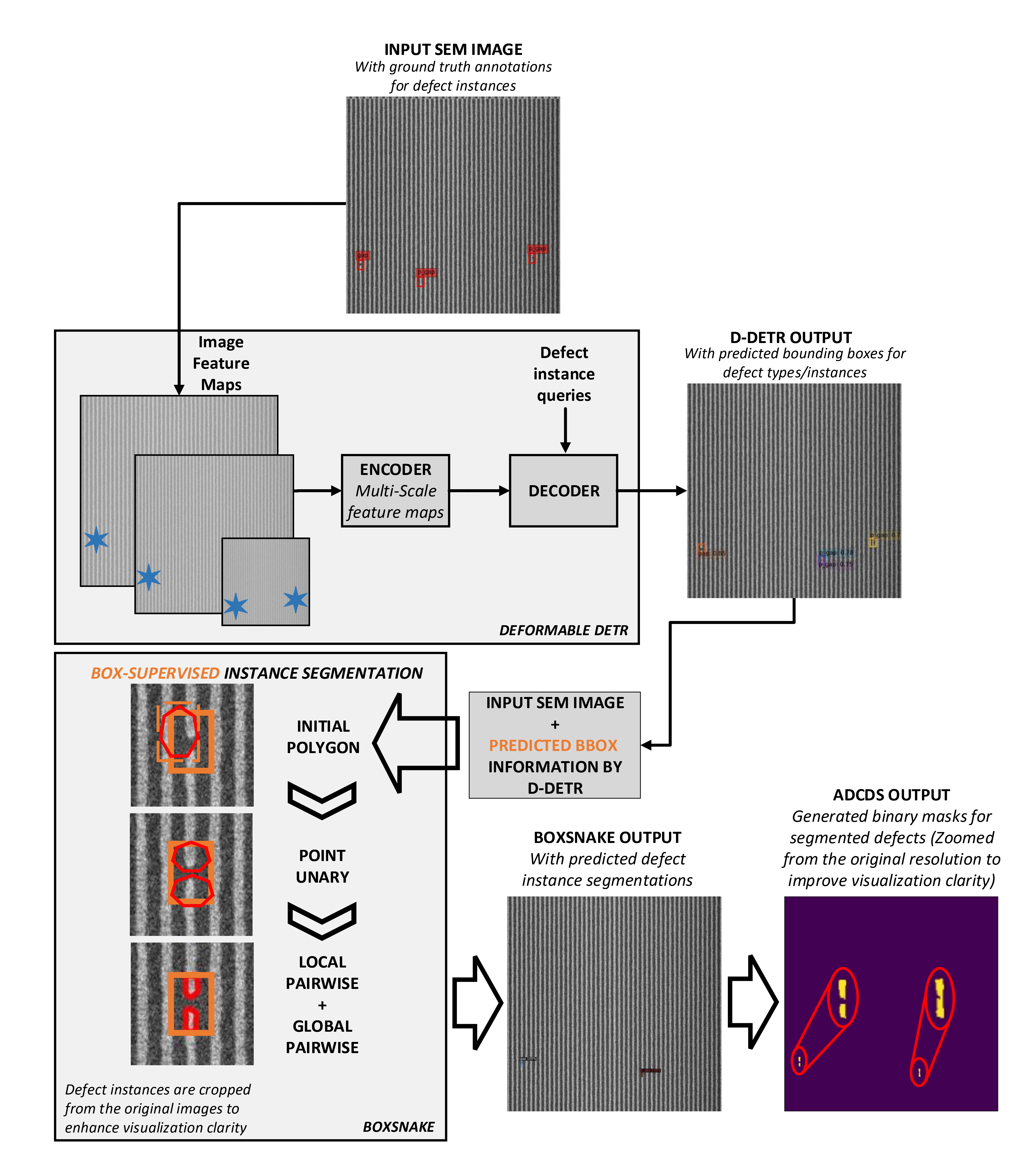
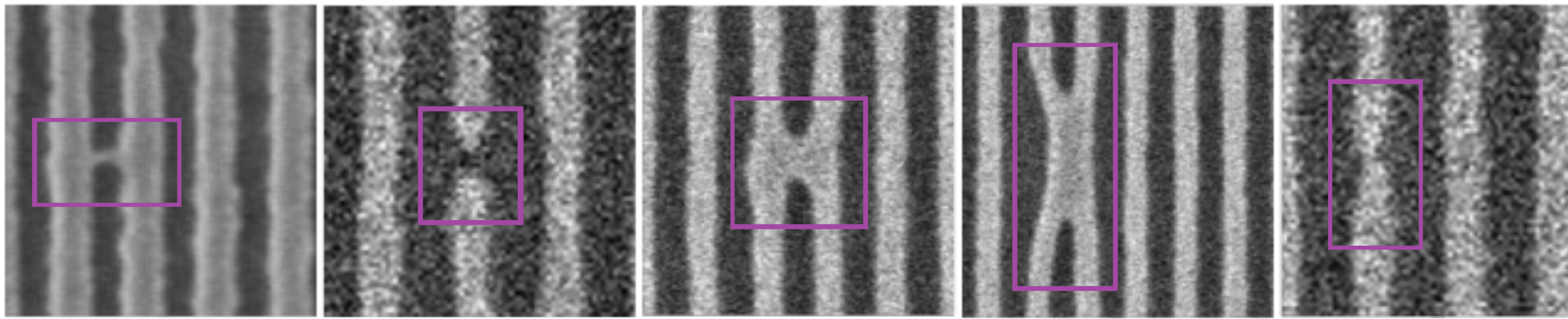
In this research, we introduce a unified end-to-end Automated Defect Classification-Detection-Segmentation (ADCDS) framework for classifying, detecting, and segmenting multiple instances of semiconductor defects for advanced nodes. This framework consists of two modules: (a) a defect detection module, followed by (b) a defect segmentation module. The defect detection module employs Deformable DETR to aid in the classification and detection of nano-scale defects, while the segmentation module utilizes BoxSnake. BoxSnake facilitates box-supervised instance segmentation of nano-scale defects, supported by the former module. This simplifies the process by eliminating the laborious requirement for ground-truth pixel-wise mask annotation by human experts, which is typically associated with training conventional segmentation models. We have evaluated the performance of our ADCDS framework using two distinct process datasets from real wafers, as ADI and AEI, specifically focusing on Line-space patterns. We have demonstrated the applicability and significance of our proposed methodology, particularly in the nano-scale segmentation and generation of binary defect masks, using the challenging ADI SEM dataset where ground-truth pixelwise segmentation annotations were unavailable. Furthermore, we have presented a comparative analysis of our proposed framework against previous approaches to demonstrate its effectiveness. Our proposed framework achieved an overall [email protected] of 72.19 for detection and 78.86 for segmentation on the ADI dataset. Similarly, for the AEI dataset, these metrics were 90.38 for detection and 95.48 for segmentation. Thus, our proposed framework effectively fulfils the requirements of advanced defect analysis while addressing significant constraints.
Read more9/9/2024

0
Addressing Class Imbalance and Data Limitations in Advanced Node Semiconductor Defect Inspection: A Generative Approach for SEM Images
Bappaditya Dey, Vic De Ridder, Victor Blanco, Sandip Halder, Bartel Van Waeyenberge
Precision in identifying nanometer-scale device-killer defects is crucial in both semiconductor research and development as well as in production processes. The effectiveness of existing ML-based approaches in this context is largely limited by the scarcity of data, as the production of real semiconductor wafer data for training these models involves high financial and time costs. Moreover, the existing simulation methods fall short of replicating images with identical noise characteristics, surface roughness and stochastic variations at advanced nodes. We propose a method for generating synthetic semiconductor SEM images using a diffusion model within a limited data regime. In contrast to images generated through conventional simulation methods, SEM images generated through our proposed DL method closely resemble real SEM images, replicating their noise characteristics and surface roughness adaptively. Our main contributions, which are validated on three different real semiconductor datasets, are: i) proposing a patch-based generative framework utilizing DDPM to create SEM images with intended defect classes, addressing challenges related to class-imbalance and data insufficiency, ii) demonstrating generated synthetic images closely resemble real SEM images acquired from the tool, preserving all imaging conditions and metrology characteristics without any metadata supervision, iii) demonstrating a defect detector trained on generated defect dataset, either independently or combined with a limited real dataset, can achieve similar or improved performance on real wafer SEM images during validation/testing compared to exclusive training on a real defect dataset, iv) demonstrating the ability of the proposed approach to transfer defect types, critical dimensions, and imaging conditions from one specified CD/Pitch and metrology specifications to another, thereby highlighting its versatility.
Read more7/16/2024
0
An Evaluation of Continual Learning for Advanced Node Semiconductor Defect Inspection
Amit Prasad, Bappaditya Dey, Victor Blanco, Sandip Halder
Deep learning-based semiconductor defect inspection has gained traction in recent years, offering a powerful and versatile approach that provides high accuracy, adaptability, and efficiency in detecting and classifying nano-scale defects. However, semiconductor manufacturing processes are continually evolving, leading to the emergence of new types of defects over time. This presents a significant challenge for conventional supervised defect detectors, as they may suffer from catastrophic forgetting when trained on new defect datasets, potentially compromising performance on previously learned tasks. An alternative approach involves the constant storage of previously trained datasets alongside pre-trained model versions, which can be utilized for (re-)training from scratch or fine-tuning whenever encountering a new defect dataset. However, adhering to such a storage template is impractical in terms of size, particularly when considering High-Volume Manufacturing (HVM). Additionally, semiconductor defect datasets, especially those encompassing stochastic defects, are often limited and expensive to obtain, thus lacking sufficient representation of the entire universal set of defectivity. This work introduces a task-agnostic, meta-learning approach aimed at addressing this challenge, which enables the incremental addition of new defect classes and scales to create a more robust and generalized model for semiconductor defect inspection. We have benchmarked our approach using real resist-wafer SEM (Scanning Electron Microscopy) datasets for two process steps, ADI and AEI, demonstrating its superior performance compared to conventional supervised training methods.
Read more7/18/2024