Addressing Class Imbalance and Data Limitations in Advanced Node Semiconductor Defect Inspection: A Generative Approach for SEM Images

0

Sign in to get full access
Overview
- This paper addresses the challenges of class imbalance and data limitations in semiconductor defect inspection using scanning electron microscope (SEM) images.
- The researchers propose a generative approach based on Diffusion Probabilistic Models (DPMs) to generate synthetic defect images and improve the performance of defect detection and classification models.
- The paper demonstrates the effectiveness of this approach in improving the robustness and accuracy of semiconductor defect inspection systems.
Plain English Explanation
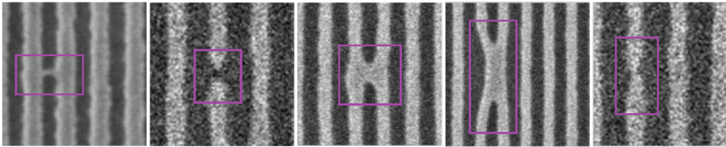
In the semiconductor industry, inspecting and classifying defects on silicon wafers is a critical step to ensure product quality. However, this task can be challenging due to several factors, including an imbalance in the number of defect types observed and a limited amount of training data for rare defect types.
To address these issues, the researchers in this paper explored the use of a generative AI model called a Diffusion Probabilistic Model (DPM) to generate synthetic SEM images of semiconductor defects. The idea is that by creating additional training data for the less common defect types, the machine learning models used for defect detection and classification can become more robust and accurate.
The DPM-based approach works by learning the underlying patterns and distributions in the real SEM images, and then using that knowledge to generate new, realistic-looking defect images. This can help overcome the limitations of traditional data augmentation techniques and improve the performance of AI-guided defect detection systems.
The researchers demonstrated the effectiveness of their approach through experiments on real-world SEM image datasets, showing that the generated images can significantly improve the accuracy of defect classification models, especially for the less common defect types.
Technical Explanation
The key technical elements of this paper are:
-
Diffusion Probabilistic Models (DPMs): The researchers used a DPM-based generative approach to synthesize new SEM images of semiconductor defects. DPMs are a class of generative models that learn to convert simple noise distributions into complex data distributions, such as natural images.
-
Defect Classification Architecture: The paper proposes a deep learning-based defect classification architecture that takes the generated SEM images as input, along with the real SEM images, to improve the performance of defect detection and classification.
-
Experimental Evaluation: The researchers evaluated their approach on real-world SEM image datasets, comparing the performance of the defect classification model with and without the generated synthetic images. They showed that the use of synthetic data can significantly improve the classification accuracy, especially for the minority defect classes.
-
Insights and Discussions: The paper provides insights into the challenges of semiconductor defect inspection, such as the inherent class imbalance in the data and the limited availability of training samples for rare defect types. It also discusses the potential of generative AI approaches, like DPMs, to address these issues and improve the robustness of defect inspection systems.
Critical Analysis
The paper presents a promising approach to addressing the challenges of class imbalance and data limitations in semiconductor defect inspection. The use of DPM-based synthesis to generate additional training data for minority defect classes is a novel and well-executed idea.
However, the paper does not delve deeply into the limitations of the proposed approach. For example, it would be valuable to understand the computational complexity and training time required for the DPM model, as well as the potential sensitivity of the approach to the quality and diversity of the real-world training data.
Additionally, the paper could have discussed the potential for further improving the generative model through techniques like contrastive learning or combining it with other data augmentation strategies.
Overall, the research presented in this paper is a valuable contribution to the field of semiconductor defect inspection, and the DPM-based approach shows promise for enhancing the performance of AI-powered defect detection and classification systems.
Conclusion
This paper addresses a critical challenge in the semiconductor industry by proposing a generative approach to overcome the limitations of class imbalance and data scarcity in semiconductor defect inspection. The use of Diffusion Probabilistic Models to synthesize realistic SEM images of defects, and the integration of these generated images into the defect classification pipeline, demonstrates a novel and effective solution to improve the robustness and accuracy of defect detection and classification systems.
The findings of this research have the potential to significantly impact the semiconductor manufacturing process, leading to enhanced product quality, reduced costs, and improved overall efficiency. As the semiconductor industry continues to push the boundaries of technology, the insights and techniques presented in this paper will be invaluable in ensuring the reliable and accurate inspection of advanced semiconductor devices.
This summary was produced with help from an AI and may contain inaccuracies - check out the links to read the original source documents!
Related Papers
0
Addressing Class Imbalance and Data Limitations in Advanced Node Semiconductor Defect Inspection: A Generative Approach for SEM Images
Bappaditya Dey, Vic De Ridder, Victor Blanco, Sandip Halder, Bartel Van Waeyenberge
Precision in identifying nanometer-scale device-killer defects is crucial in both semiconductor research and development as well as in production processes. The effectiveness of existing ML-based approaches in this context is largely limited by the scarcity of data, as the production of real semiconductor wafer data for training these models involves high financial and time costs. Moreover, the existing simulation methods fall short of replicating images with identical noise characteristics, surface roughness and stochastic variations at advanced nodes. We propose a method for generating synthetic semiconductor SEM images using a diffusion model within a limited data regime. In contrast to images generated through conventional simulation methods, SEM images generated through our proposed DL method closely resemble real SEM images, replicating their noise characteristics and surface roughness adaptively. Our main contributions, which are validated on three different real semiconductor datasets, are: i) proposing a patch-based generative framework utilizing DDPM to create SEM images with intended defect classes, addressing challenges related to class-imbalance and data insufficiency, ii) demonstrating generated synthetic images closely resemble real SEM images acquired from the tool, preserving all imaging conditions and metrology characteristics without any metadata supervision, iii) demonstrating a defect detector trained on generated defect dataset, either independently or combined with a limited real dataset, can achieve similar or improved performance on real wafer SEM images during validation/testing compared to exclusive training on a real defect dataset, iv) demonstrating the ability of the proposed approach to transfer defect types, critical dimensions, and imaging conditions from one specified CD/Pitch and metrology specifications to another, thereby highlighting its versatility.
Read more7/16/2024
0
An Evaluation of Continual Learning for Advanced Node Semiconductor Defect Inspection
Amit Prasad, Bappaditya Dey, Victor Blanco, Sandip Halder
Deep learning-based semiconductor defect inspection has gained traction in recent years, offering a powerful and versatile approach that provides high accuracy, adaptability, and efficiency in detecting and classifying nano-scale defects. However, semiconductor manufacturing processes are continually evolving, leading to the emergence of new types of defects over time. This presents a significant challenge for conventional supervised defect detectors, as they may suffer from catastrophic forgetting when trained on new defect datasets, potentially compromising performance on previously learned tasks. An alternative approach involves the constant storage of previously trained datasets alongside pre-trained model versions, which can be utilized for (re-)training from scratch or fine-tuning whenever encountering a new defect dataset. However, adhering to such a storage template is impractical in terms of size, particularly when considering High-Volume Manufacturing (HVM). Additionally, semiconductor defect datasets, especially those encompassing stochastic defects, are often limited and expensive to obtain, thus lacking sufficient representation of the entire universal set of defectivity. This work introduces a task-agnostic, meta-learning approach aimed at addressing this challenge, which enables the incremental addition of new defect classes and scales to create a more robust and generalized model for semiconductor defect inspection. We have benchmarked our approach using real resist-wafer SEM (Scanning Electron Microscopy) datasets for two process steps, ADI and AEI, demonstrating its superior performance compared to conventional supervised training methods.
Read more7/18/2024

0
Towards Improved Semiconductor Defect Inspection for high-NA EUVL based on SEMI-SuperYOLO-NAS
Ying-Lin Chen, Jacob Deforce, Vic De Ridder, Bappaditya Dey, Victor Blanco, Sandip Halder, Philippe Leray
Due to potential pitch reduction, the semiconductor industry is adopting High-NA EUVL technology. However, its low depth of focus presents challenges for High Volume Manufacturing. To address this, suppliers are exploring thinner photoresists and new underlayers/hardmasks. These may suffer from poor SNR, complicating defect detection. Vision-based ML algorithms offer a promising solution for semiconductor defect inspection. However, developing a robust ML model across various image resolutions without explicit training remains a challenge for nano-scale defect inspection. This research's goal is to propose a scale-invariant ADCD framework capable to upscale images, addressing this issue. We propose an improvised ADCD framework as SEMI-SuperYOLO-NAS, which builds upon the baseline YOLO-NAS architecture. This framework integrates a SR assisted branch to aid in learning HR features by the defect detection backbone, particularly for detecting nano-scale defect instances from LR images. Additionally, the SR-assisted branch can recursively generate upscaled images from their corresponding downscaled counterparts, enabling defect detection inference across various image resolutions without requiring explicit training. Moreover, we investigate improved data augmentation strategy aimed at generating diverse and realistic training datasets to enhance model performance. We have evaluated our proposed approach using two original FAB datasets obtained from two distinct processes and captured using two different imaging tools. Finally, we demonstrate zero-shot inference for our model on a new, originating from a process condition distinct from the training dataset and possessing different Pitch characteristics. Experimental validation demonstrates that our proposed ADCD framework aids in increasing the throughput of imaging tools for defect inspection by reducing the required image pixel resolutions.
Read more4/10/2024

0
Utilizing Generative Adversarial Networks for Image Data Augmentation and Classification of Semiconductor Wafer Dicing Induced Defects
Zhining Hu, Tobias Schlosser, Michael Friedrich, Andr'e Luiz Vieira e Silva, Frederik Beuth, Danny Kowerko
In semiconductor manufacturing, the wafer dicing process is central yet vulnerable to defects that significantly impair yield - the proportion of defect-free chips. Deep neural networks are the current state of the art in (semi-)automated visual inspection. However, they are notoriously known to require a particularly large amount of data for model training. To address these challenges, we explore the application of generative adversarial networks (GAN) for image data augmentation and classification of semiconductor wafer dicing induced defects to enhance the variety and balance of training data for visual inspection systems. With this approach, synthetic yet realistic images are generated that mimic real-world dicing defects. We employ three different GAN variants for high-resolution image synthesis: Deep Convolutional GAN (DCGAN), CycleGAN, and StyleGAN3. Our work-in-progress results demonstrate that improved classification accuracies can be obtained, showing an average improvement of up to 23.1 % from 65.1 % (baseline experiment) to 88.2 % (DCGAN experiment) in balanced accuracy, which may enable yield optimization in production.
Read more7/31/2024