AI-Guided Defect Detection Techniques to Model Single Crystal Diamond Growth

0
🔎
Sign in to get full access
Overview
- Diamond growth via chemical vapor deposition has made significant progress, but challenges remain in achieving high-quality, large-area material production.
- Controlling conditions to maintain uniform growth rates across the entire growth surface is a key challenge.
- As growth progresses, various factors or defect states emerge, altering the uniform conditions and affecting the growth rate, leading to microscale crystalline defects.
- There is a lack of methods to identify these defect states and their geometry using in-situ optical images during the growth process.
Plain English Explanation
The paper focuses on the challenge of producing high-quality, large-scale diamond materials using a process called chemical vapor deposition (CVD). In this process, diamond is grown by exposing a surface to a gas mixture that contains the necessary ingredients for diamond formation.
One of the main obstacles is maintaining consistent growth conditions across the entire surface being grown. As the diamond grows, various issues or "defect states" can arise, disrupting the uniform conditions and causing problems like uneven growth rates and tiny crystalline defects. These defects are problematic and can impact the diamond's quality.
Unfortunately, there hasn't been a good way to identify these defect states and their shapes using the live optical images captured during the growth process. This is an important capability to have, as it could help researchers and engineers better understand and control the CVD diamond growth process.
Technical Explanation
The paper presents a novel approach to defect segmentation pipeline using in-situ optical images to identify features that indicate defective states visible at the macroscale. The researchers used a semantic segmentation approach to isolate and classify these defect states and their corresponding derivative features by their pixel masks.
To efficiently produce training datasets, the team developed a human-in-the-loop software architecture with modules for selective data labeling using active learning, data augmentations, and model-assisted labeling. This drastically reduced the time and cost of labeling compared to traditional methods.
For the machine learning models, the researchers found that deep learning-based algorithms were the most efficient, as they could accurately learn complex representations from the feature-rich datasets. Their best-performing model, based on the YOLOV3 and DeeplabV3plus architectures, achieved excellent accuracy for specific defect features of interest, reaching over 90% accuracy for center, polycrystalline, and edge defects.
Critical Analysis
The paper presents a comprehensive approach to addressing a crucial challenge in the diamond CVD growth process. However, the researchers acknowledge that the method is limited to 2D in-situ optical images, and there may be additional defect states or features that are not visible in these images.
Further research could explore the integration of other sensing modalities, such as 3D scanning or spectroscopy, to provide a more comprehensive understanding of the defect states and their effects on the growth process. Additionally, the performance of the deep learning models could potentially be improved by incorporating advanced techniques like few-shot learning or zero-shot segmentation.
Overall, the work presented in this paper represents a significant step forward in addressing a critical challenge in the production of high-quality, large-scale diamond materials using CVD. The novel defect segmentation pipeline and the insights gained from the machine learning models provide a solid foundation for further advancements in this field.
Conclusion
This paper details a pioneering approach to identifying defect states during the chemical vapor deposition (CVD) growth of diamond materials. By developing a defect segmentation pipeline using in-situ optical images and leveraging state-of-the-art deep learning models, the researchers have made substantial progress in addressing a longstanding challenge in this field.
The ability to accurately detect and classify these defect states is crucial for improving the quality and scalability of CVD diamond production, which has numerous applications in various industries, from electronics to optics. The insights and techniques presented in this work pave the way for further advancements in the understanding and control of the diamond growth process, ultimately contributing to the development of high-performance diamond materials with widespread impact.
This summary was produced with help from an AI and may contain inaccuracies - check out the links to read the original source documents!
Related Papers
🔎
0
AI-Guided Defect Detection Techniques to Model Single Crystal Diamond Growth
Rohan Reddy Mekala, Elias Garratt, Matthias Muehle, Arjun Srinivasan, Adam Porter, Mikael Lindvall
From a process development perspective, diamond growth via chemical vapor deposition has made significant strides. However, challenges persist in achieving high quality and large-area material production. These difficulties include controlling conditions to maintain uniform growth rates for the entire growth surface. As growth progresses, various factors or defect states emerge, altering the uniform conditions. These changes affect the growth rate and result in the formation of crystalline defects at the microscale. However, there is a distinct lack of methods to identify these defect states and their geometry using images taken during the growth process. This paper details seminal work on defect segmentation pipeline using in-situ optical images to identify features that indicate defective states that are visible at the macroscale. Using a semantic segmentation approach as applied in our previous work, these defect states and corresponding derivative features are isolated and classified by their pixel masks. Using an annotation focused human-in-the-loop software architecture to produce training datasets, with modules for selective data labeling using active learning, data augmentations, and model-assisted labeling, our approach achieves effective annotation accuracy and drastically reduces the time and cost of labeling by orders of magnitude. On the model development front, we found that deep learning-based algorithms are the most efficient. They can accurately learn complex representations from feature-rich datasets. Our best-performing model, based on the YOLOV3 and DeeplabV3plus architectures, achieved excellent accuracy for specific features of interest. Specifically, it reached 93.35% accuracy for center defects, 92.83% for polycrystalline defects, and 91.98% for edge defects.
Read more4/12/2024
✨
0
AI-Guided Feature Segmentation Techniques to Model Features from Single Crystal Diamond Growth
Rohan Reddy Mekala, Elias Garratt, Matthias Muehle, Arjun Srinivasan, Adam Porter, Mikael Lindvall
Process refinement to consistently produce high-quality material over a large area of the grown crystal, enabling various applications from optics crystals to quantum detectors, has long been a goal for diamond growth. Machine learning offers a promising path toward this goal, but faces challenges such as the complexity of features within datasets, their time-dependency, and the volume of data produced per growth run. Accurate spatial feature extraction from image to image for real-time monitoring of diamond growth is crucial yet complicated due to the low-volume and high feature complexity nature of the datasets. This paper compares various traditional and machine learning-driven approaches for feature extraction in the diamond growth domain, proposing a novel deep learning-driven semantic segmentation approach to isolate and classify accurate pixel masks of geometric features like diamond, pocket holder, and background, along with their derivative features based on shape and size. Using an annotation-focused human-in-the-loop software architecture for training datasets, with modules for selective data labeling using active learning, data augmentations, and model-assisted labeling, our approach achieves effective annotation accuracy and drastically reduces labeling time and cost. Deep learning algorithms prove highly efficient in accurately learning complex representations from datasets with many features. Our top-performing model, based on the DeeplabV3plus architecture, achieves outstanding accuracy in classifying features of interest, with accuracies of 96.31% for pocket holder, 98.60% for diamond top, and 91.64% for diamond side features.
Read more4/15/2024
0
An Evaluation of Continual Learning for Advanced Node Semiconductor Defect Inspection
Amit Prasad, Bappaditya Dey, Victor Blanco, Sandip Halder
Deep learning-based semiconductor defect inspection has gained traction in recent years, offering a powerful and versatile approach that provides high accuracy, adaptability, and efficiency in detecting and classifying nano-scale defects. However, semiconductor manufacturing processes are continually evolving, leading to the emergence of new types of defects over time. This presents a significant challenge for conventional supervised defect detectors, as they may suffer from catastrophic forgetting when trained on new defect datasets, potentially compromising performance on previously learned tasks. An alternative approach involves the constant storage of previously trained datasets alongside pre-trained model versions, which can be utilized for (re-)training from scratch or fine-tuning whenever encountering a new defect dataset. However, adhering to such a storage template is impractical in terms of size, particularly when considering High-Volume Manufacturing (HVM). Additionally, semiconductor defect datasets, especially those encompassing stochastic defects, are often limited and expensive to obtain, thus lacking sufficient representation of the entire universal set of defectivity. This work introduces a task-agnostic, meta-learning approach aimed at addressing this challenge, which enables the incremental addition of new defect classes and scales to create a more robust and generalized model for semiconductor defect inspection. We have benchmarked our approach using real resist-wafer SEM (Scanning Electron Microscopy) datasets for two process steps, ADI and AEI, demonstrating its superior performance compared to conventional supervised training methods.
Read more7/18/2024
0
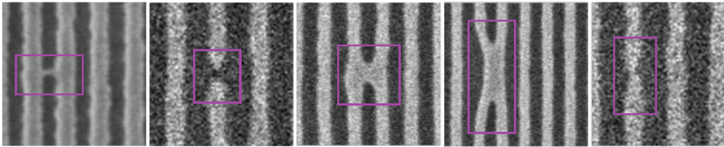
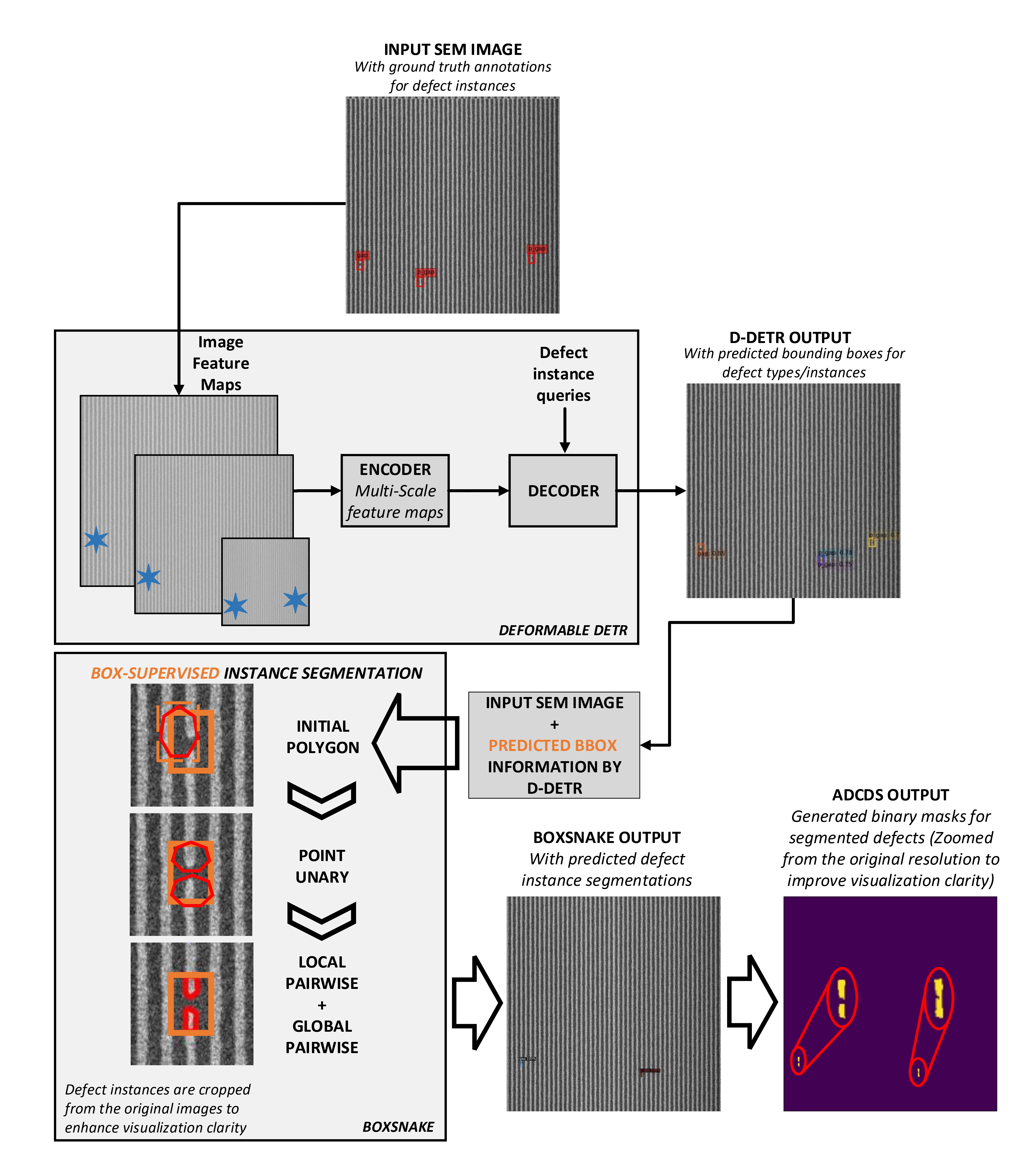
Advancing SEM Based Nano-Scale Defect Analysis in Semiconductor Manufacturing for Advanced IC Nodes
Bappaditya Dey, Matthias Monden, Victor Blanco, Sandip Halder, Stefan De Gendt
In this research, we introduce a unified end-to-end Automated Defect Classification-Detection-Segmentation (ADCDS) framework for classifying, detecting, and segmenting multiple instances of semiconductor defects for advanced nodes. This framework consists of two modules: (a) a defect detection module, followed by (b) a defect segmentation module. The defect detection module employs Deformable DETR to aid in the classification and detection of nano-scale defects, while the segmentation module utilizes BoxSnake. BoxSnake facilitates box-supervised instance segmentation of nano-scale defects, supported by the former module. This simplifies the process by eliminating the laborious requirement for ground-truth pixel-wise mask annotation by human experts, which is typically associated with training conventional segmentation models. We have evaluated the performance of our ADCDS framework using two distinct process datasets from real wafers, as ADI and AEI, specifically focusing on Line-space patterns. We have demonstrated the applicability and significance of our proposed methodology, particularly in the nano-scale segmentation and generation of binary defect masks, using the challenging ADI SEM dataset where ground-truth pixelwise segmentation annotations were unavailable. Furthermore, we have presented a comparative analysis of our proposed framework against previous approaches to demonstrate its effectiveness. Our proposed framework achieved an overall [email protected] of 72.19 for detection and 78.86 for segmentation on the ADI dataset. Similarly, for the AEI dataset, these metrics were 90.38 for detection and 95.48 for segmentation. Thus, our proposed framework effectively fulfils the requirements of advanced defect analysis while addressing significant constraints.
Read more9/9/2024