Enhancing Printed Circuit Board Defect Detection through Ensemble Learning

0

Sign in to get full access
Overview
- This paper proposes an ensemble learning approach to enhance the detection of defects in printed circuit boards (PCBs).
- The researchers developed a multi-model ensemble that combines the strengths of different deep learning models to improve the accuracy and robustness of PCB defect detection.
- The ensemble approach was evaluated on a large dataset of PCB images, demonstrating significant improvements over individual models.
Plain English Explanation
The paper discusses a way to improve the detection of defects, or flaws, in printed circuit boards (PCBs) using a technique called ensemble learning. Printed circuit boards are the foundational components that power many of our electronic devices, like computers and phones. It's important to be able to detect any defects in these boards during the manufacturing process to ensure the devices work properly.
The researchers tried combining the results from several different deep learning models, which are advanced AI algorithms that can analyze images and identify patterns. By combining the outputs from multiple models, the researchers were able to create a more accurate and reliable system for detecting defects in the PCB images. This ensemble approach takes advantage of the unique strengths of each individual model to get better overall performance.
The team tested their ensemble method on a large dataset of PCB images and found that it significantly outperformed the individual models working alone. This suggests that the ensemble approach is a promising way to enhance PCB defect detection and help ensure the quality and reliability of the electronic devices we rely on every day.
Technical Explanation
The paper proposes an ensemble learning approach to improve the detection of defects in printed circuit boards (PCBs). The researchers developed a multi-model ensemble that combines the outputs of different deep learning models, including Faster R-CNN, YOLOv5, and Mask R-CNN.
The ensemble architecture first extracts visual features from the input PCB images using a shared backbone network. These features are then passed to the individual detection models, which produce bounding boxes and segmentation masks for any detected defects. The outputs from the models are combined using a weighted averaging scheme to produce the final ensemble prediction.
The researchers evaluated the proposed ensemble method on a large dataset of PCB images, comparing its performance to the individual deep learning models. The results showed that the ensemble approach significantly outperformed the individual models in terms of precision, recall, and F1-score, demonstrating the benefits of leveraging the complementary strengths of multiple models.
Critical Analysis
The paper provides a thorough evaluation of the ensemble learning approach, including detailed comparisons to the individual deep learning models. However, the authors do not address potential limitations or areas for further research.
One potential concern is the computational cost and complexity of the ensemble approach, which may limit its practicality for real-time deployment in industrial settings. The paper does not provide any analysis of the runtime or resource requirements of the ensemble model.
Additionally, the dataset used in the evaluation is not publicly available, which makes it difficult for other researchers to validate the results or extend the work. Providing a publicly available dataset would help advance the field of PCB defect detection research.
Conclusion
This paper presents a novel ensemble learning approach to enhance the detection of defects in printed circuit boards. The proposed multi-model ensemble leverages the complementary strengths of different deep learning architectures to achieve superior performance over individual models.
The results demonstrate the potential of ensemble methods to improve the reliability and robustness of PCB defect detection, which is crucial for ensuring the quality and safety of electronic devices. While the paper does not address all potential limitations, it represents an important step forward in this important area of research.
This summary was produced with help from an AI and may contain inaccuracies - check out the links to read the original source documents!
Related Papers
0
Enhancing Printed Circuit Board Defect Detection through Ensemble Learning
Ka Nam Canaan Law, Mingshuo Yu, Lianglei Zhang, Yiyi Zhang, Peng Xu, Jerry Gao, Jun Liu
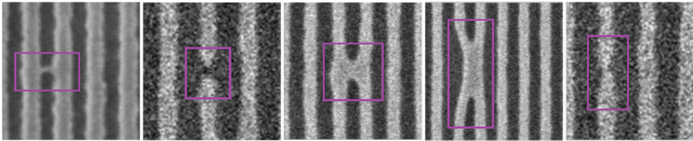
The quality control of printed circuit boards (PCBs) is paramount in advancing electronic device technology. While numerous machine learning methodologies have been utilized to augment defect detection efficiency and accuracy, previous studies have predominantly focused on optimizing individual models for specific defect types, often overlooking the potential synergies between different approaches. This paper introduces a comprehensive inspection framework leveraging an ensemble learning strategy to address this gap. Initially, we utilize four distinct PCB defect detection models utilizing state-of-the-art methods: EfficientDet, MobileNet SSDv2, Faster RCNN, and YOLOv5. Each method is capable of identifying PCB defects independently. Subsequently, we integrate these models into an ensemble learning framework to enhance detection performance. A comparative analysis reveals that our ensemble learning framework significantly outperforms individual methods, achieving a 95% accuracy in detecting diverse PCB defects. These findings underscore the efficacy of our proposed ensemble learning framework in enhancing PCB quality control processes.
Read more9/17/2024

0
YOLO-pdd: A Novel Multi-scale PCB Defect Detection Method Using Deep Representations with Sequential Images
Bowen Liu, Dongjie Chen, Xiao Qi
With the rapid growth of the PCB manufacturing industry, there is an increasing demand for computer vision inspection to detect defects during production. Improving the accuracy and generalization of PCB defect detection models remains a significant challenge. This paper proposes a high-precision, robust, and real-time end-to-end method for PCB defect detection based on deep Convolutional Neural Networks (CNN). Traditional methods often suffer from low accuracy and limited applicability. We propose a novel approach combining YOLOv5 and multiscale modules for hierarchical residual-like connections. In PCB defect detection, noise can confuse the background and small targets. The YOLOv5 model provides a strong foundation with its real-time processing and accurate object detection capabilities. The multi-scale module extends traditional approaches by incorporating hierarchical residual-like connections within a single block, enabling multiscale feature extraction. This plug-and-play module significantly enhances performance by extracting features at multiple scales and levels, which are useful for identifying defects of varying sizes and complexities. Our multi-scale architecture integrates feature extraction, defect localization, and classification into a unified network. Experiments on a large-scale PCB dataset demonstrate significant improvements in precision, recall, and F1-score compared to existing methods. This work advances computer vision inspection for PCB defect detection, providing a reliable solution for high-precision, robust, real-time, and domain-adaptive defect detection in the PCB manufacturing industry.
Read more7/23/2024
0
An Evaluation of Continual Learning for Advanced Node Semiconductor Defect Inspection
Amit Prasad, Bappaditya Dey, Victor Blanco, Sandip Halder
Deep learning-based semiconductor defect inspection has gained traction in recent years, offering a powerful and versatile approach that provides high accuracy, adaptability, and efficiency in detecting and classifying nano-scale defects. However, semiconductor manufacturing processes are continually evolving, leading to the emergence of new types of defects over time. This presents a significant challenge for conventional supervised defect detectors, as they may suffer from catastrophic forgetting when trained on new defect datasets, potentially compromising performance on previously learned tasks. An alternative approach involves the constant storage of previously trained datasets alongside pre-trained model versions, which can be utilized for (re-)training from scratch or fine-tuning whenever encountering a new defect dataset. However, adhering to such a storage template is impractical in terms of size, particularly when considering High-Volume Manufacturing (HVM). Additionally, semiconductor defect datasets, especially those encompassing stochastic defects, are often limited and expensive to obtain, thus lacking sufficient representation of the entire universal set of defectivity. This work introduces a task-agnostic, meta-learning approach aimed at addressing this challenge, which enables the incremental addition of new defect classes and scales to create a more robust and generalized model for semiconductor defect inspection. We have benchmarked our approach using real resist-wafer SEM (Scanning Electron Microscopy) datasets for two process steps, ADI and AEI, demonstrating its superior performance compared to conventional supervised training methods.
Read more7/18/2024

0
Towards Improved Semiconductor Defect Inspection for high-NA EUVL based on SEMI-SuperYOLO-NAS
Ying-Lin Chen, Jacob Deforce, Vic De Ridder, Bappaditya Dey, Victor Blanco, Sandip Halder, Philippe Leray
Due to potential pitch reduction, the semiconductor industry is adopting High-NA EUVL technology. However, its low depth of focus presents challenges for High Volume Manufacturing. To address this, suppliers are exploring thinner photoresists and new underlayers/hardmasks. These may suffer from poor SNR, complicating defect detection. Vision-based ML algorithms offer a promising solution for semiconductor defect inspection. However, developing a robust ML model across various image resolutions without explicit training remains a challenge for nano-scale defect inspection. This research's goal is to propose a scale-invariant ADCD framework capable to upscale images, addressing this issue. We propose an improvised ADCD framework as SEMI-SuperYOLO-NAS, which builds upon the baseline YOLO-NAS architecture. This framework integrates a SR assisted branch to aid in learning HR features by the defect detection backbone, particularly for detecting nano-scale defect instances from LR images. Additionally, the SR-assisted branch can recursively generate upscaled images from their corresponding downscaled counterparts, enabling defect detection inference across various image resolutions without requiring explicit training. Moreover, we investigate improved data augmentation strategy aimed at generating diverse and realistic training datasets to enhance model performance. We have evaluated our proposed approach using two original FAB datasets obtained from two distinct processes and captured using two different imaging tools. Finally, we demonstrate zero-shot inference for our model on a new, originating from a process condition distinct from the training dataset and possessing different Pitch characteristics. Experimental validation demonstrates that our proposed ADCD framework aids in increasing the throughput of imaging tools for defect inspection by reducing the required image pixel resolutions.
Read more4/10/2024